In the world of electronics, understanding the differences between single-sided and multi-layer PCBs is crucial for selecting the right printed circuit board for specific applications. Single-sided PCBs offer simplicity and cost-effectiveness, while multi-layer PCBs provide enhanced functionality and compact design, catering to advanced technological needs. Companies like OurPCB – https://www.ourpcb.com, a renowned pcb manufacturer, offer a range of options to suit various requirements, ensuring that you can find the ideal PCB solution for your project.
Overview of PCBs
Printed Circuit Boards (PCBs) play a crucial role in modern electronics. They provide mechanical support and electrical connections for electronic components. A PCB consists of a substrate, conductive pathways, and solder mask, which ensures proper functioning in devices.
Different types of PCBs cater to specific applications. Single-sided PCBs offer simplicity and cost-effectiveness, making them suitable for basic electronic devices like calculators and timers. In contrast, multi-layer PCBs comprise multiple layers of conductive material, facilitating complex circuit designs for advanced applications in telecommunications, automotive, and medical devices.
- Single-Sided PCBs: These consist of one conductive layer and are ideal for straightforward electronic designs. They are often favored for their low manufacturing costs and ease of mass production.
- Multi-Layer PCBs: These boards include three or more conductive layers, enabling high-density circuits. They accommodate more components within a smaller footprint, which is essential for compact and intricate designs.
Manufacturers provide diverse PCB solutions, including standard, high-frequency, and aluminum PCBs, tailored to different industry requirements. Understanding these distinctions aids in selecting the right PCB type for specific project needs.
Single-Sided PCBs
Single-sided PCBs, or single-layer PCBs, feature components and conductive copper on one side, with the wiring located on the opposite side. Their structure includes a substrate layer, a conductive metal layer, a protective solder mask, and a silkscreen.
Definition and Structure
A single-sided PCB primarily consists of a single layer of conductive material, allowing for straightforward circuit designs. The substrate provides the base for mounting electronic components. The conductive metal layer allows for electrical connections, while the solder mask protects the circuitry. This design simplifies manufacturing and facilitates easier component placement, making it suitable for basic electronic devices.
Advantages and Disadvantages
Advantages
- Lower Cost: Single-sided PCBs typically cost less to produce due to their simple design and fewer materials compared to multi-layer PCBs.
- Easier to Design and Produce: They require less design time and fewer resources during the manufacturing process.
- Facilitate Mass Production: The simplicity allows for easy reproduction in large quantities, lowering the cost per unit.
- Shorter Delivery Times: Quick manufacturing processes make them ideal for projects that need fast turnaround.
- Limited Functionality: Single-sided PCBs may not support complex designs, restricting their use to basic applications.
- Space Constraints: The single layer can limit the number of components that can be mounted, impacting circuit density.
- Less Durability: Single-sided designs may be less robust than multi-layer options, making them less suitable for demanding environments.
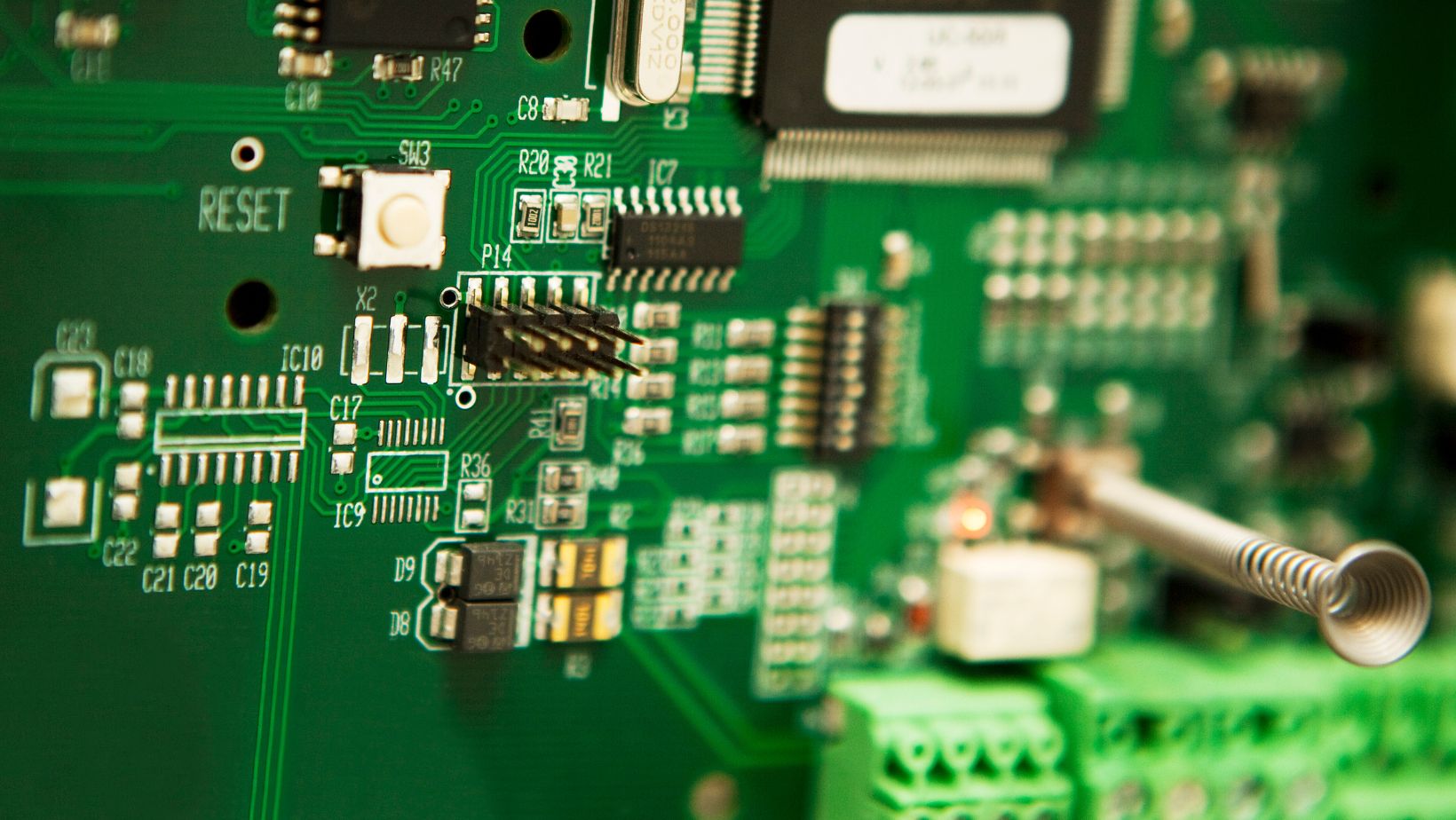
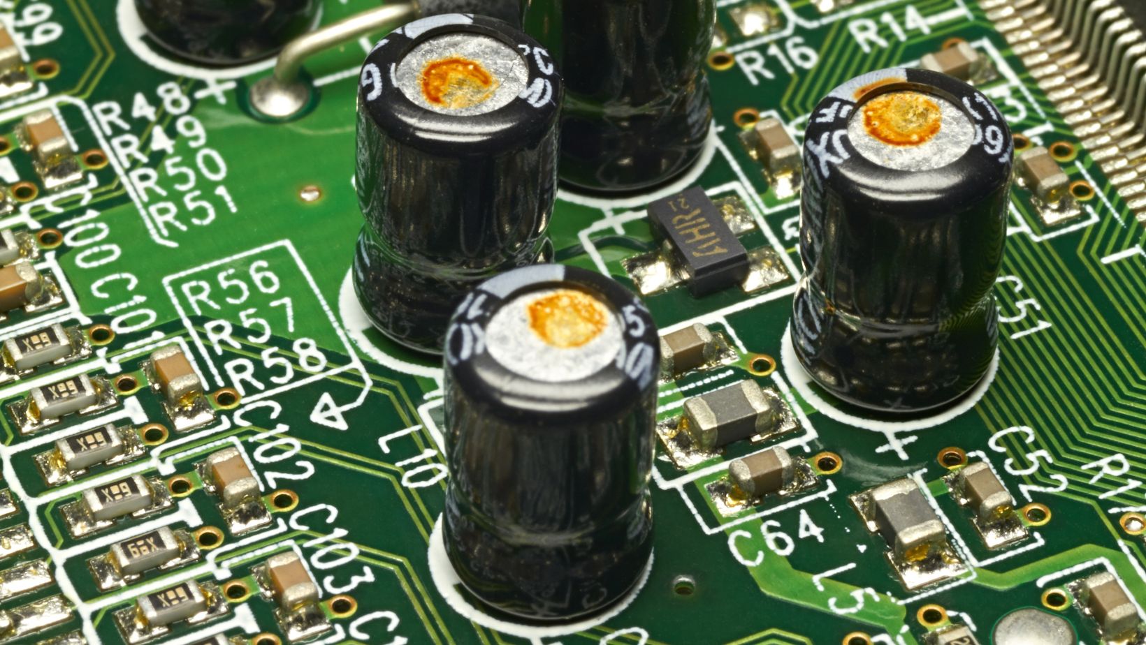
Multi-Layer PCBs
Multi-layer PCBs consist of several layers of conductive material, typically copper, separated by insulation. These boards are created by stacking multiple double-sided PCBs with insulation layers, allowing for more complex circuit designs.
Definition and Structure
Multi-layer PCBs range from four to twelve layers, though designs with up to 129 layers exist. Each layer has distinct roles; for instance, some layers handle power distribution while others focus on signal processing. Insulation prevents short circuiting between layers, ensuring stable performance.
Advanced manufacturing techniques create these PCBs, incorporating precision and high-quality materials to improve durability and performance.
Advantages and Disadvantages
Multi-layer PCBs offer significant advantages, including:
- Increased Design Flexibility: They accommodate complex configurations and numerous connections, making them ideal for sophisticated electronic devices.
- Enhanced Performance: Multi-layer designs enable higher operational speeds and capacities compared to single-sided PCBs, supporting advanced functionalities.
- Improved Quality: The production process requires specialized skills, resulting in higher quality boards tailored to specific applications.
- Durability: These boards are generally more robust and lighter than their single-sided counterparts, enhancing their efficiency in various environments.
Despite their benefits, multi-layer PCBs present challenges:
- Higher Costs: The production process is more expensive, making them less suitable for low-budget projects.
- Manufacturing Complexity: The intricate design and assembly processes require advanced technology and expertise.
Identifying the right application depends on balancing these pros and cons with the specific project requirements.
Key Differences Between Single-Sided and Multi-Layer PCBs
Single-sided and multi-layer PCBs differ significantly in cost, complexity, and application suitability.
Cost Considerations
Single-sided PCBs offer affordability, making them an economical choice for mass production. Production involves fewer resources, less time, and reduced expertise. Multi-layer PCBs incur higher costs due to their complex design, which requires more materials and intricate manufacturing processes.
Complexity and Design
Single-sided PCBs feature one layer of conductive material, ideal for low-density circuit designs. They are simpler to design and produce, limiting space for components. Multi-layer PCBs consist of multiple layers of conductive materials insulated from one another, enabling support for complex circuit designs. This complexity results in enhanced flexibility and performance, meeting diverse technological needs.
Applications
Single-sided PCBs serve applications like basic consumer electronics, where simple functionality is enough. Multi-layer PCBs find use in advanced technology sectors, including telecommunications for high-frequency communication devices, automotive for durable electronics, medical devices requiring high precision, and consumer electronics demanding performance. The choice between them aligns with specific project requirements and application environments.
Conclusion
Choosing between single-sided and multi-layer PCBs hinges on the specific needs of a project. Single-sided PCBs excel in cost-effectiveness and simplicity making them a go-to for basic applications.
Multi-layer PCBs however provide the advanced capabilities necessary for complex designs and high-performance requirements. Understanding the differences in cost complexity and application suitability helps in making informed decisions. Ultimately the right choice ensures that the electronic device meets its intended performance and reliability standards.